
Products

CST118A
CST118A outputs a peak DC current of 2.5A and a continuous current of 1.8A, with a power supply operating range of 2V-6V.
CST118A has a set of PWM (INA-INB) inputs, low output resistance, and is packaged in SOP8.
CST118ASummary:
CST118A is a single channel DC brushed motor driver IC, suitable for electronic locks, electric toothbrushes, toys, consumer products, and other low-voltage or battery powered motion control products.
CST118A outputs a peak DC current of 2.5A and a continuous current of 1.8A, with a power supply operating range of 2V-6V.
CST118A has a set of PWM (INA-INB) inputs, low output resistance, and is packaged in SOP8.
CST118AFeature:
Single channel built-in power MOS full bridge driver
Working voltage range: 2V-6V
Drive forward, backward, stop and brake functions
Low on resistance: high side+low side (HS+LS=400mΩ)
Built in hysteresis heating effect overheat protection function
The maximum continuous output current can reach 1.8A, with a peak value of 2.5A
No need for large peripheral filtering capacitors, only small surface mount capacitors are needed
Adopting SOP-8 encapsulation format
CST118AApplication:
Electronic lock
Electric toothbrush
CST118AOrdering Instructions:
PartNo.
|
Package
|
Mark*
|
Tape/Reel
|
CST118A
|
SOP8
|
CST-LOGO-CST118A
TXXXXXX
|
4000PCS/卷
|
118A(中性标)
|
SOP8
|
118A
XXXXXX
|
4000PCS/卷
|
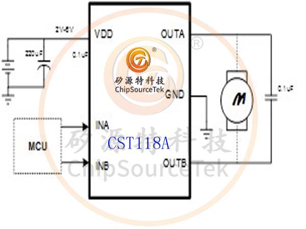
CST118ATypical schematic diagram:

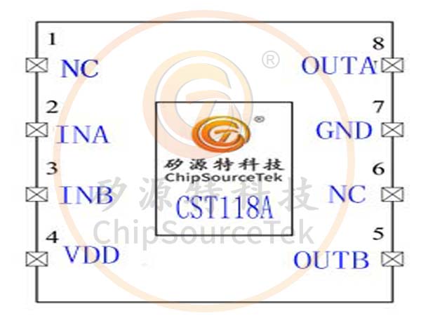
CST118APin diagram and pin description:

|
Number
|
Name
|
IO
|
Pin Descripation
|
1
|
NC
|
-
|
Hanging in the air
|
|
2
|
INA
|
I
|
Combining INB to determine output status
|
|
3
|
INB
|
I
|
Determine the output status based on INA
|
|
4
|
VDD
|
P
|
Power Supply
|
|
5
|
OUTB
|
O
|
Full bridge output B terminal
|
|
6
|
NC
|
-
|
Suspended or grounded
|
|
7
|
GND
|
P
|
land
|
|
8
|
OUTA
|
O
|
Full bridge output A terminal
|
CST118ALimit parameter:(Note1)
Symbol
|
Explain
|
Value
|
Company
|
|
Voltage
|
Power supply voltage (VDD)
|
6.0
|
V
|
|
Maximum continuous output current
|
1.2
|
A
|
||
Peak output current
|
2
|
A
|
||
Power waste
|
Pd
|
SOP8
|
0.96
|
W
|
Thermal resistance
|
ӨJA
|
SOP8
|
130
|
oC/W
|
TJ
|
Range of junction temperature
|
-40 to +150
|
oC
|
|
TSTG
|
Storage temperature range
|
-40 to +150
|
||
TSDR
|
Welding temperature range
|
260
|
||
Note 1. Absolute maximum rated value refers to the value at which the lifespan of the device may be damaged, which may cause permanent damage to the chip under absolute maximum rated conditions.
Symbol
|
Explain
|
Minimum value
|
Maximum value
|
Company
|
VDD
|
Supply Voltage
|
2.0
|
6
|
V
|
VI
|
Logic input voltage range
|
0
|
VDD
|
|
IOUT
|
Forward and reverse current
|
-1.8
|
1.8
|
A
|
CST118A Electrical Characteristics:
(Unless otherwise specified, TA=25 ℃, VCC=3V, RL=15Ω)
Parameter
|
Symbol
|
Test conditions
|
Minimum value
|
Typical values
|
Maximum value
|
Company
|
|
Whole
|
|||||||
ICCST
|
Turn off the current
|
INA=INB=GND
|
━
|
0
|
10
|
uA
|
|
ICC
|
静态电流
|
INA=H,INB=L
INA=L,INB=H
INA=H,INB=H
|
━
|
0.3
|
1
|
mA
|
|
Control input
|
|||||||
VINH
|
高电平输入电压
|
2.0
|
━
|
━
|
V
|
||
VINL
|
低电平输入电压
|
━
|
━
|
0.8
|
V
|
||
IINH
|
高电平输入电流
|
VIN = 3V
|
━
|
5
|
20
|
uA
|
|
IINL
|
低电平输入电流
|
VIN = 0V
|
-1
|
0
|
━
|
uA
|
|
RIN
|
下拉电阻
|
━
|
1.5
|
━
|
MΩ
|
||
Drive
|
|||||||
RON
|
输出导通阻抗
|
IO = 200mA
|
0.4
|
Ω
|
|||
RPLD
|
INA、INB内置下拉电阻
|
150
|
kΩ
|
||||
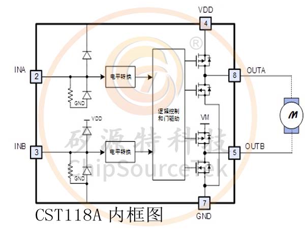
CST118A内部框图:
CST118A输入/输出逻辑表:
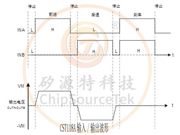
输入
|
Output
|
Method
|
||
INA
|
INB
|
OUTA
|
OUTB
|
|
L
|
L
|
Hi-Z
|
Hi-Z
|
Standby status
|
H
|
L
|
H
|
L
|
Forward
|
L
|
H
|
L
|
H
|
Back off
|
H
|
H
|
L
|
L
|
刹车
|
CST118A输入/输出波形:

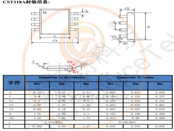
CST118A封装信息:


Please submit your basic information, send an email to[email protected], or call us at 13823761625 (same number as WeChat), and we will contact you as soon as possible!

WeChat Official Account

WeChat Service
 Email
Email
 QQ
QQ
 13823761625

